Cadence Virtuoso:: Design of NAND Gate Schematic || Part-1.
ANALOG DESIGN OF NAND GATE||CMOS VLSI||Using Virtuoso schematic editor||Virtuoso ADE||Spectre||VTU
How to draw schematic diagram for 2input CMOS NAND GATE
CMOS NAND Gate
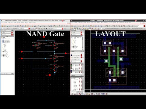
Schematic diagram and layout of two input NAND gate
Cadence Virtuoso:: Layout of NAND Gate || Part-2.
Schematic Diagram for 4 to 1 Counter Circuit (using NAND Gates 7400N)
NAND Gate Schematic & Layout.
9. Drawing the schematic and icon of a NAND gate
Design and Simulation of a NAND Gate using Tanner
バックエンド ラボ 3 : NAND ゲート
NANDゲートを使用したSRラッチ回路
NAND ゲート - 基本とチュートリアル
Design of NAND Gate Schematic in Cadence Virtuoso #cadence #virtuoso #vlsi #vlsidesign
L-17: NAND Gate schematic design using Tanner EDA tool
CMOS 2-input NAND and NOR gates | Layout diagram | VLSI | Lec-34
Transistor Logic Gates - NAND, AND, OR, NOR
Cadence Virtuoso での CMOS NAND ゲートの回路図、シンボル、およびシミュレーション
NAND ゲート トランジスタの設計と CMOS ゲート アレイの実装
Making logic gates from transistors