stick diagram of CMOS inverter || clear explanation ||Explore the way
CMOS inverter | Layout diagram | VLSI | Lec-33
Layout of CMOS INVERTER using P-WELL Process || Explore the way
CMOS inverter | Stick diagram | VLSI | Lec-27
Stick diagram of CMOS Inverter
CMOS Inverter Stick and Mask layout diagrams, Stick and layout diagrams,how to design stick diagrams
Stick diagram of a Boolean function || Explore the way
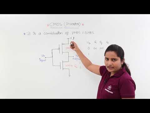
CMOS Inverter
Stick Diagram of Boolean Function | CMOS Boolean Function Circuit | VLSI by Engineering Funda
EC 304 VLSI |Stick Diagram| CMOS inverter| CMOS NAND|CMOS NOR| Malayalam
Cmos inverter - logic,stick,layout diagram
CMOS inverter layout
スティックダイアグラムの描き方 (VLSI)|簡略化|例付き
CMOS 2-input NAND and NOR gates | Layout diagram | VLSI | Lec-34
how to draw stick diagram and layout diagram in VLSI
CMOS Inverter Stick Diagram
Cadence Virtuoso:: CMOS Inverter Layout || Part-2.
Stick Diagram for CMOS Inverter
stick diagram of two input CMOS nand gate || compact stick diagram || Explore the way
CMOS Inverter-STick diagram/Layout