3.3 PCB Layer
Multilayer PCB Stack-up Basics | PCB Knowledge
basic tutorials for beginners for EasyEDA | simplest circuit simulation tutorial in EasyEDA
How to use Easyeda | Basics
Innovative PCB Shapes: EasyEDA Tutorial + @JLCPCB Order Guide for Custom Designs
Learn Something New! Using EasyEDA to design custom circuit boards
Creating PCBs with EasyEDA
Why is 50 OHM impedance used in PCB Layout? | Explained | Eric Bogatin | #HighlightsRF
How to Learn EasyEDA under 60 mins! | 2023 | #pcbcupid
What are Mounting Holes? | PCB Knowledge
DIY Soldering Station #2 - PCB Design with EasyEDA
Using Fusion 360 To Design A Case For PCB That Was Designed In EasyEDA
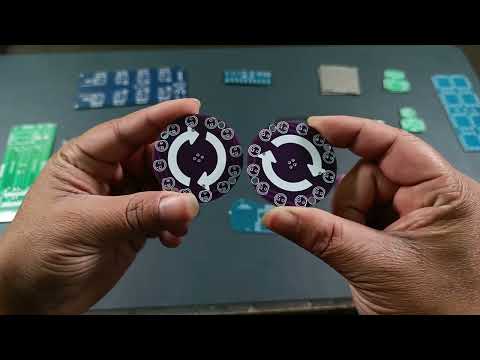
My First PCB Design 😃 #pcb #shorts
Top 5 Beginner PCB Design Mistakes (and how to fix them)
PCB設計者としてオンラインで収入を得る方法 | PCB設計でオンラインで収入を得る | Easyedaで稼ぐ
What are PCBs? || How do PCBs Work?
How to export files from easyeda | How to manage PCB Layout print in MS Word | PCB board layout
PCB DESIGN Part -2
Creating pcb trace fuse links in EasyEDA
#165 From Schematic to PCB - Part 2: Designing and Ordering the PCB ✅