How does a diode work - the PN Junction (with animation) | Intermediate Electronics
Formation and Properties of Junction Diode - Physics
Diffusion, drift & barrier voltage | Class 12 (India) | Physics | Khan Academy
P-N JUNCTION
PN Junction Introduction
P-N Junction Diode and Depletion Layer, Chapter 14, Semiconductor Electronics, Class 12 Physics
PN junction Diode Explained | Forward Bias and Reverse Bias
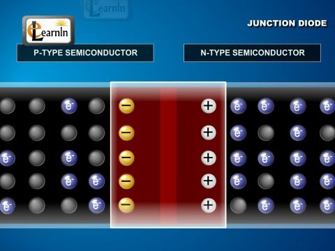
Depletion Region
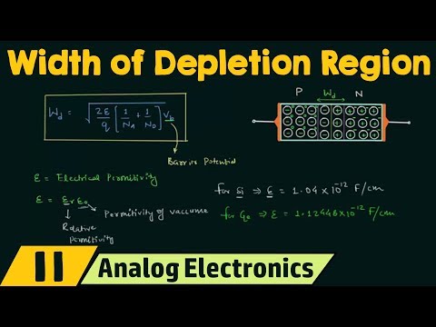
Width of Depletion Region
p-n Junction Diode (Part 1) || Depletion Region | Barrier Potential | Semiconductor - 08 || in HINDI
The PN junction | Class 12 (India) | Physics | Khan Academy
Formation of Depletion layer, Barrier voltage and Biasing in PN junction diode in English
Formation of Depletion Layer - Semiconductor Physics - Diploma Physics 1
What do you mean by depletion layer?
formation of depletion layer in PN junction
Formation of Depletion Layer and Potential Barrier| SEMICONDUCTOR DEVICES| PHYSICS |
Derivation of Width of depletion layer| Electronics||✓
p n junction (depletion region and energy bands)
Introduction to P-N Junction Diode and Formation of Depletion Region - Basic Electronics
PN Junction Diode working in Tamil