ASIC Design Flow | RTL to GDS | Chip Design Flow
FPGA Design Flow: 7 Essential Steps to Implementing a Circuit on an FPGA
ASIC Design Flow | How a chip is designed??
8.16. FPGA design flow
Lecture 3: FPGA design flow and EDA
What is ASIC - FPGA - SoC? | Explanation, Differences & Applications
ASIC Design Flow I Physical Design
ASIC Design Flow Deep Dive Part 1
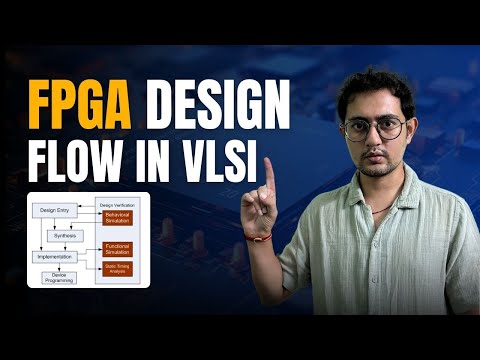
VLSI FOR Beginners - FPGA Design Flow in VLSI | How it is different from ASIC Design Flow ?
Introduction to VLSI - IC Design Flow | ASIC Design Flow | RTL to GDS Flow | Chip Design Flow
The Ultimate Guide to FPGA Development Tools | What is VHDL Design Flow ?
Day 2 – ASIC Design Flow Explained | 50 Days Verilog Challenge #vlsi #verilog #asicdesignflow
VLSI Design Flow || specification to GDS2 ||Both FPGA and ASIC design flow || what exactly is GDSII
FPGA Design Flow
VLSI FOR ALL - ASIC & FPGA 設計フロー、HDL 言語の必要性、Verilog の基礎とデータ型 | チュートリアル
ASIC Design Flow in VLSI Design || Learn Thought || S Vijay Murugan
The ASIC DESIGN FLOW Secret That's CHANGING THE GAME | CHIPVERSE
ASIC Design Flow | Application Specific Integrated Circuit | VLSI Design | SoC (system-on-chip)
Vivek De Introduces ASIC Design Flow