ASIC Design Flow | RTL to GDS | Chip Design Flow
ASIC Design Flow | How a chip is designed??
What is ASIC - FPGA - SoC? | Explanation, Differences & Applications
VLSI ASIC Design flow
What is an ASIC?
Introduction to VLSI - IC Design Flow | ASIC Design Flow | RTL to GDS Flow | Chip Design Flow
ASIC Design | Introduction | Simplified VLSI KTU ECT 304 S6 |
FPGAとは何ですか?
ASIC Design Flow
VLSI ASIC Design Flow | ASIC Flow | Physical Design Flow | Back end design flow | RTL 2 GDS flow
What is a Application Specific Integrated Circuit ASIC
Physical Design Flow | VLSI back end | IC Design
Overview of Frontend Design Flow in VLSI | VLSI -IC Design Flow | ASIC Design Flow |RTL to GDS Flow
What is the full custom ASIC design | VLSI interview Questions and Answers
What is TIMING ECO | VLSI | ASIC DESIGN | PHYSICAL DESIGN | VLSIFaB
ASIC vs FPGA | Qualcomm Interview Questions🔥
VLSI Physical Design Detailed Roadmap | Analog Design Career | VLSI POINT
仕様からシリコンまで: ASIC 設計フローをステップバイステップで説明します。
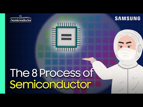
‘Semiconductor Manufacturing Process’ Explained | 'All About Semiconductor' by Samsung Semiconductor
What Is the AMS Top-Down Design Flow?