ASIC Design Flow | RTL to GDS | Chip Design Flow
ASIC Design Flow | How a chip is designed??
Open Source Analog ASIC design: Entire Process
ASIC Design Flow - Part 1
Learn ASIC design with the 1-minute MOSFET
ASIC Design Flow in VLSI Design || Learn Thought || S Vijay Murugan
What is ASIC - FPGA - SoC? | Explanation, Differences & Applications
Introduction to VLSI - IC Design Flow | ASIC Design Flow | RTL to GDS Flow | Chip Design Flow
What is TIMING ECO | VLSI | ASIC DESIGN | PHYSICAL DESIGN | VLSIFaB
ASIC Design Course Welcome
You Know❓ASIC Design Flow is really EASY | Job opportunities | EDA Tools used
ASIC Design Flow
究極のVLSIロードマップ | 半導体業界への参入方法 | プロジェクト | 無料リソース📚
What is an ASIC?
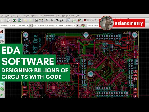
Designing Billions of Circuits with Code
VLSI Physical Design Detailed Roadmap | Analog Design Career | VLSI POINT
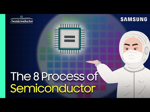
‘Semiconductor Manufacturing Process’ Explained | 'All About Semiconductor' by Samsung Semiconductor
ASIC Design Flow (Front-end vs Back-end)
VLSI ASIC Design flow
How To Design and Manufacture Your Own Chip