How To Create Your Own Libraries in Altium Designer
CADSTAR PCB シンボルとフットプリント
005 回路図シンボルの作成
複数のピン テーブル BGA シンボルとフットプリント | OrCAD PCB デザイナー
シンボルとフットプリントの作成 | Altium Designer - Phil's Lab #31
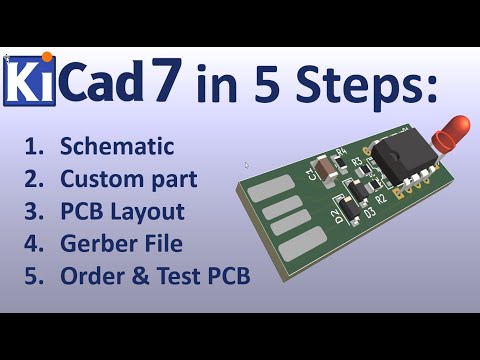
KiCAD 7 PCB Layout in 5 steps
Altium Designer チュートリアル 9 : AD 21 ライブラリでテスト ポイント シンボルとフットプリントを作成する方法。
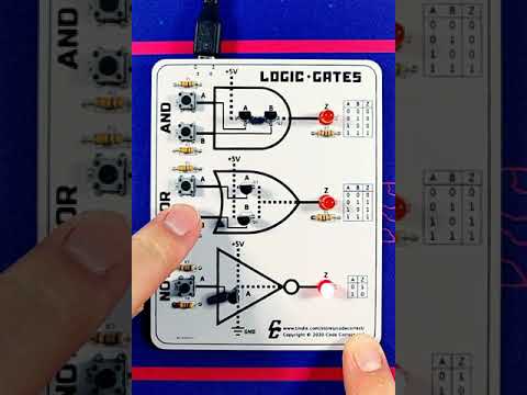
Logic Gates Learning Kit #2 - Transistor Demo
レーザー加工機でオリジナルプリント基板作り Homemade PCB with laser cutter
Creating Schematic Symbols & Footprint Libraries in Altium Designer
Working with Pin Groups in BGA Schematic Symbols
How to Use ADCs in the PCB
Electrical quantities units symbol | SI units #shorts #viral #trending #electrical #trending
Senior Programmers vs Junior Developers #shorts
ALTIUM TUTORIAL-24: How To Draw Custom Pad/Design LED PCB 3535/3030/2835/DESIGN CIRCULAR PAD
Mechanical engineering best interview✓
How to Place Embedded Cavities in a PCB
ECU DCM 1.2 READING & WRITING FLASH
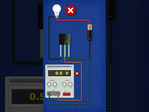
Transistors Explained - What is a transistor?
Resistor Color Code #shorts #shortvideo #viralvideo