VLSI design flow (Basics, Flowchart, Domains & Y Chart) Explained | VLSI by Engineering Funda
Introduction to VLSI - IC Design Flow | ASIC Design Flow | RTL to GDS Flow | Chip Design Flow
ASIC Design Flow | RTL to GDS | Chip Design Flow
What is VLSI | Introduction & Design flow | VLSI | Lec-01
VLSI Design Flow|VLSI |Engineering|Btech|ECE|JNTUA|Sem|spmvv|Telugu|MWE|in English
ASIC Design Flow in VLSI Design || Learn Thought || S Vijay Murugan
Verilog HDL (18EC56) | Typical HDL Design flow | VTU
VLSI Design Flow || Unit 1: Ch.2
VLSI DESIGN FLOW
What is VLSI Design Flow REALLY About?
ASIC design flow in VLSI
VLSI Terminologies (Hierarchy, Regularity, Modularity & Locality) Explained
ASIC Design | Introduction | Simplified VLSI KTU ECT 304 S6 |
BIST - Built In Self Test (Basics, Types, Architecture, Working, Challenges, Pros & Cons) Explained
CMOSラムダベースの設計ルール || VLSI設計 || S VIJAY MURUGAN || 思考を学ぶ
VLSI design Methodologies | Types of VLSI Design | VLSI Technology window | Engineering Funda
Modeling Style in VHDL || VLSI Unit1 ch. 3
FPGA design flow | Block Diagram | VLSI | Lec-74
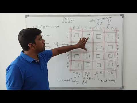
FPGA ( Field Programmable Gate Array ) - Simplified | Circuit | VLSI KTU
VLSI設計におけるフィールドプログラマブルゲートアレイ || Learn Thought || S Vijay Murugan