Cadence. Transfer characteristic (I-V) MOSFET by tran analysis
DC 注釈: Cadence の MOS の領域、Vth、Id、Vgs、Ron、gm。
Experiment 6: JK Flip flop using Static cmos gates Cadence virtuoso
Virtuoso での D フリップフロップの回路図設計。
Cadence Virtuoso: CMOS インバータのプロセスコーナー分析。
VLSIプロジェクト: Cadence VirtuosoによるCMOS電流コンパレータの設計とシミュレーション
Cadence Virtuoso: NOR ゲートのレイアウト || パート 2。
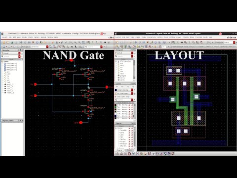
Cadence Virtuoso:: Layout of NAND Gate || Part-2.
cadence simulation tutorial of digital design | verilog code simulation in cadence tool |VLSI design
Cadence Virtuoso tool for the design of CMOS inverter | Cadence tutorial | DC & Transient Analysis
Cadence Virtuoso でのモンテカルロ解析。
nand schematic design using CADENCE VIRTUOSO
3-Input NOR gate designing and run in Cadence Virtuso.VLSI
Cadence AC Simulation (Low Pass Filter)
CMOS Inverter (NOT Gate): Schematic and Symbol #cadence #virtuoso
Cmos based MUX design and simulate part 1 | Cadence
CMOS D Flip Flop | Schematic | Symbol | Transient response | Cadence Virtuoso
Design of CMOS Transmission Gates using Cadence Virtuoso | CMOS circuits #VLSI_Design
Introduction to Layout design in Cadence Virtuoso
D-Latch & D-Flip flop.