Mask layout | Lambda based design rules | VLSI | Lec-32
5つのレイアウト設計ルールの説明 モジュール2 6学期 VLSI ECE VTU
インバータ、NAND、NOR、式の9つのレイアウトの説明 モジュール4 6学期 VLSI設計とテスト EC VTU
How to design a layout design rules in vlsi on Tanner ?
CMOSインバータ | レイアウト図 | VLSI | Lec-33
Want to become successful Chip Designer ? #vlsi #chipdesign #icdesign
CMOS logic functions | Layout diagram | VLSI | Lec-35
Stick diagrams | Rules to draw | VLSI | Lec-26
Stick diagrams | MOS layers | VLSI | Lec-24
Design Rule Check Seedstudio
CMOS | 2入力NANDゲートとNORゲート | レイアウト図 | VLSI | Lec-34
Length of Diffusion LOD:A Key Concept in Analog layout design Matching with prevention @Job_seeker
Top 6 VLSI Project Ideas for Electronics Engineering Students 🚀💡
6つのラムダベースPウェル設計ルールの説明 モジュール2 6学期 VLSI ECE VTU
Free PCB Design Software
ALIGN Installation Guide || Setting Up Automatic Layout Generator || VLSI Layout Tools
MOS Layout layers | Color Coding | Representation | VLSI | Lec-31
How to include additional rule files in Calibre Interactive
Download CMOS VLSI Design: A Circuits and Systems Perspective (4th Edition) PDF
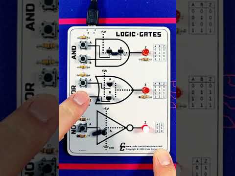
Logic Gates Learning Kit #2 - Transistor Demo