「半導体製造プロセス」の解説 | サムスンセミコンダクター「半導体のすべて」
#300mmシリコン#ウェーハ製造プロセス
ウェーハレベルパッケージング入門
半導体製造プロセスの説明
ハイブリッドボンディングがパッケージの未来である理由
300mm wafer fab virtual tour
Discover: die-to-wafer hybrid bonding | CEA-Leti
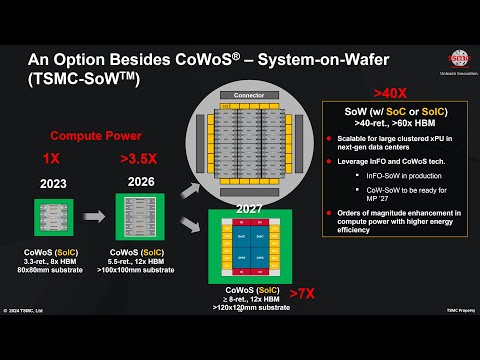
TSMC evolves CoWoS technology, to challenge 9x reticle sizes in 2027
SEMICONDUCTOR PACKAGING ASSEMBLY PROCESSES - FULL COMPILATION
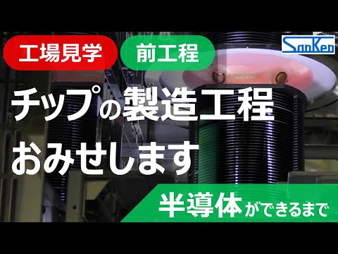
【前工程編】工場見学:半導体ができるまで|実際の製造工程を見ながらわかりやすく解説!!【サンケン電気】
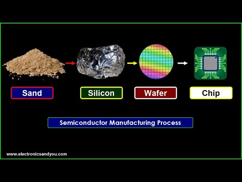
Semiconductor Manufacturing Process
SEMICONDUCTOR WAFER WET CLEANING
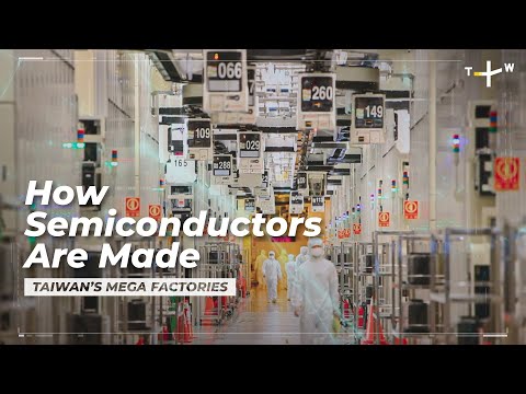
Inside Micron Taiwan’s Semiconductor Factory | Taiwan’s Mega Factories EP1
THE SEMICONDUCTOR SUPPLY CHAIN - A BRIEF OVERVIEW
Turn semiconductor manufacturing process challenges into a competitive advantage
Semiconductor Manufacturing Process Flow Chart
Discover: hybrid bonding | CEA-Leti
Photolithography: Step by step
Introduction of products for semiconductor manufacturing gas & vacuum processes
Why Wafer Bonding is the Future of Semiconductors