Introduction to VLSI - IC Design Flow | ASIC Design Flow | RTL to GDS Flow | Chip Design Flow
ASIC Design Flow | RTL to GDS | Chip Design Flow
VLSI design flow (Basics, Flowchart, Domains & Y Chart) Explained | VLSI by Engineering Funda
VLSI Design Flow|VLSI |Engineering|Btech|ECE|JNTUA|Sem|spmvv|Telugu|MWE|in English
VLSI IC DESIGN FLOW | ASIC DESIGN #btech #mtech #diploma #vlsi #icdesign #vlsidesign #vhdl #verilog
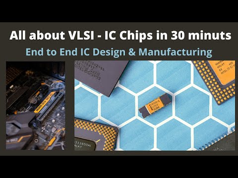
IC Design & Manufacturing Process : Beginners Overview to VLSI
Verilog HDL (18EC56) | Typical HDL Design flow | VTU
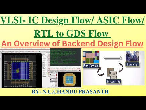
Overview of VLSI Physical Design Flow | VLSI-IC Design Flow| Netlist to GDS2 flow |PNR Flow
Physical Design Flow | VLSI back end | IC Design
ASIC Design Flow | How a chip is designed??
Chip design Flow : From concept to Product || #vlsi #chipdesign #vlsiprojects
Analog IC Design Flow: Essential Tools and Workflow
VLSI ASIC Design Flow | ASIC Flow | Physical Design Flow | Back end design flow | RTL 2 GDS flow
Want to become successful Chip Designer ? #vlsi #chipdesign #icdesign
Overview of VLSI Design Flow - I
VLSI ASIC Design flow
VLSI Design Flow | IC Design Flow |VLSI Chip Design Process | Types Of Design Process
ASIC Design Flow in VLSI Design || Learn Thought || S Vijay Murugan
Top 12 VLSI Job Roles Explained! 💡💻 | VLSI Career Paths
FPGA Design Flow: 7 Essential Steps to Implementing a Circuit on an FPGA