(Sponsored) PCB Vias 101 - Phil's Lab #77
6 Horribly Common PCB Design Mistakes
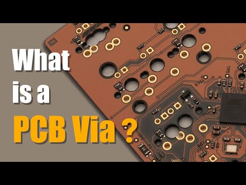
What is a PCB Via? | PCB Knowledge
What are Stitching Vias? | PCB Knowledge
スティッチングビアの深掘り | PCBレイアウト
What is PCB Via and Which Type Should You Choose ? #jlcpcb
ビアとそのアスペクト比 | PCB配線
Top 5 Beginner PCB Design Mistakes (and how to fix them)
Via-in-Pad Design | PCB Knowledge
Move Some Vias! Raspberry Pi MCU One Minute #PCBDesign Review 13 #electronics #altium
GNDビアがPCBレイアウトを改善する仕組み
Via Tenting in PCB Design. Prevent Oxidation and Failures!
What is a via used in PCB? How to design?
Demystifying Vias in High Speed PCB Design
How to Use Blind and Buried Vias
Flawless PCB design: 3 simple rules - Part 2
HDI PCB設計におけるスキップビアの統合方法
Getting Started with Blind & Buried Vias #pcbdesign #electronics #altium
To Pour or Not To Pour | Copper Pour in PCB Design
PCB Trace Design Basics | PCB Knowledge