006 Create PCB Footprint
How to Learn EasyEDA under 60 mins! | 2023 | #pcbcupid
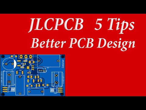
JLCPCB, Easyeda 5 tips for better PCB design
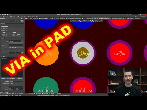
Via-in-Pad Design | PCB Knowledge
How to easily design PCB in EasyEDA software
What are Thermal Relief Pads? | PCB Knowledge
3.10 PCB Copper Pour
EasyEDA 完全チュートリアル + コンポーネントの作成 + ヒント
012 PCB Layout
Copper Regions in EasyEDA
PCB - Route - Auto Router
Using VIA in PAD? What you need to know - Guidelines, dimensions and more ...
1.9 Create Footprint
3.3 PCB Layer
How to Design a PCB from Scratch with EasyEDA | COMPLETE Tutorial | JLCPCB LCSC ALIEXPRESS | 2024
Demonstrating 'snap to pad' in EasyEDA.
How to design and create Custom Library in EasyEDA | Footprint and Schematic | PCB
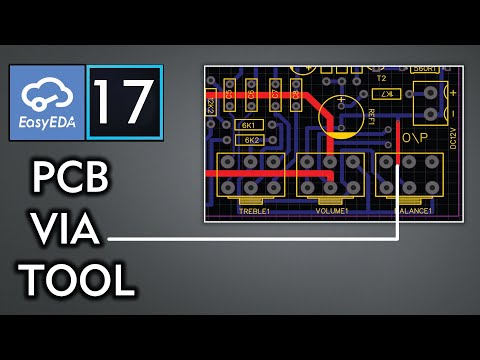
How to use Easy EDA Via Tool Class= 17 Urdu\Hindi
5. Making Pads Adjustments on EasyEDA
EasyEDA Incomplete connection? (BUT IT ISN'T!) Check this first.