VLSI Physical Design Detailed Roadmap | Analog Design Career | VLSI POINT
VLSI Physical Design Flow Overview
Physical Design Flow | VLSI back end | IC Design
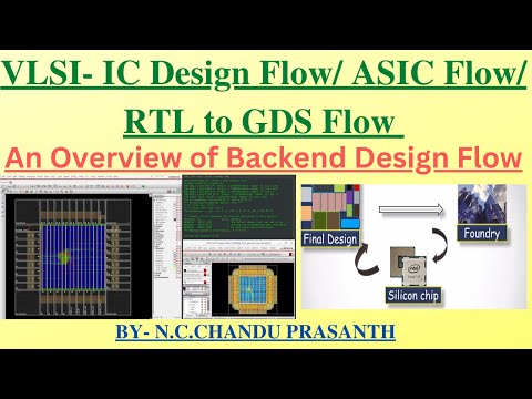
ASIC Design Flow | RTL to GDS | Chip Design Flow
Physical Design Flow Overview | VLSI interview prep for Apple Nvidia AMD Google Meta Samsung Intel
PD Lec 1 - Introduction to Physical Design | Tutorial | VLSI
Overview of VLSI Physical Design Flow |Netlist to GDS2 flow |PNR Flow
Design to Silicon: Open-Source VLSI Flow with eSim + SKY130 | The semiconductor Webinar (TSW)
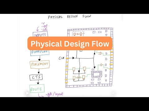
What is PHYSICAL DESIGN FLOW | FULL STEPS | VLSI
Want to become successful Chip Designer ? #vlsi #chipdesign #icdesign
VLSI design flow (Basics, Flowchart, Domains & Y Chart) Explained | VLSI by Engineering Funda
Synthesis intro (Part 1) | VLSI interview prep | Digital logic | Physical Design | Semiconductors
VLSI Backend Detailed Explanation | Backend VLSI Design Flow
VLSI ASIC Design flow
vlsi design flow in telugu || what is vlsi industry in telugu||vlsi vth prakash
Introduction to VLSI - IC Design Flow | ASIC Design Flow | RTL to GDS Flow | Chip Design Flow
All You need to know about VLSI Physical Design | Salary, Physical Design Flow, Work-Life Explained
Overview of VLSI Physical Design Flow | VLSI-IC Design Flow| Netlist to GDS2 flow |PNR Flow
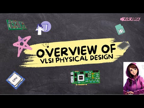
Overview of basic VLSI Physical Design flow
Basics of PHYSICAL DESIGN: Logical & Physical Synthesis Flow | Goal & Synthesis Strategies | Class-5