How to design PCB in Easyeda Pro: Introduction to Easyeda Pro for beginners
3.5 PCB Design Rules
4.6 PCB Ordering
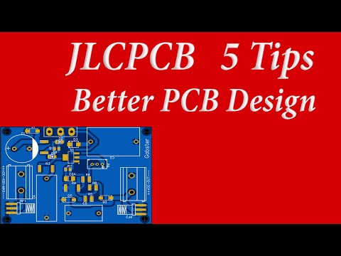
JLCPCB, Easyeda 5 tips for better PCB design
2.7 Schematic Design Rules Check
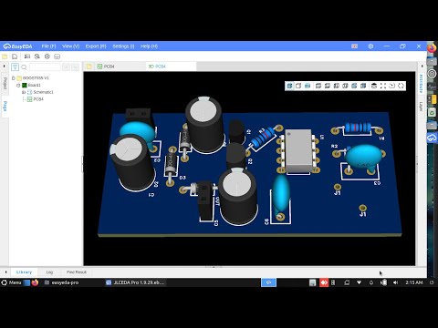
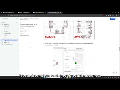
Walkthrough: Building a Small PCB in EasyEDA Pro (BGA CPLD Dev Board)
EasyEDA Live Stream
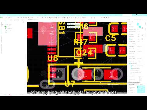
Copper Regions in EasyEDA
2.9 Reuse Block
3.1 Convert to PCB
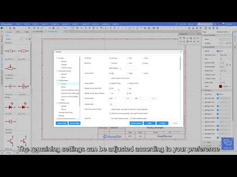
1.3 Software Settings
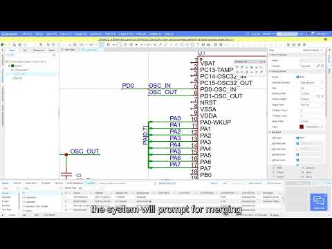
2.6 Schematic Wiring
PCB design solid region | Easyeda solid region | How to use solid region in Easyeda PCB design
3.10 PCB Copper Pour
PCB file in EasyEDA PRO ( UBUNTU )
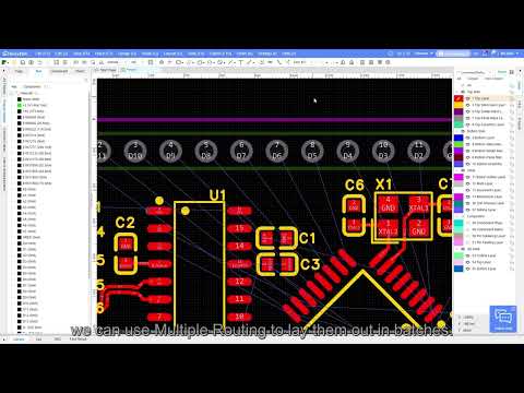
3.8 PCB Routing Skill
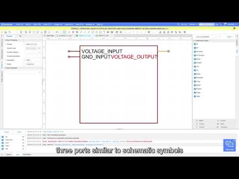
1.8 Create Component Symbol
3.14 PCB Panelization
1.1 Feature Overview
Top 10 Free 3d Modeling Softwares-EasyEDA Part 1