CMOS Circuits - Pull Down and Pull Up Network, PDN, PUN, Karnaugh Map, Digital Logic, NOT, NAND, XOR
プルアップ抵抗とプルダウン抵抗とは何ですか?プルアップ抵抗の値はどのように選択するのですか?
Short and sweet: pull up/pull down resistors explained
Why do we consider PMOS as pull up and NMOS as pull down transistor
CMOS Compound Logic | Pull-up & Pull-down
CMOS || Digital VLSI Design || Pull up and Pull down Network || CMOS Inverter || CMOS : Lecture 1
Pull ups | Load Resistor | NMOS & PMOS | VLSI | Lec-17
Electronics: What pull-up or pull-down resistors to use in CMOS logic circuits
デジタルエレクトロニクス:論理ゲート - 集積回路 パート1
CMOSの例 [Inv(A+B*C)*C+D]
What is pull down device | VLSI interview questions | ece interview questions and answers
Circuits 2 || CMOS Design: Examples to teach you how to implement any Logic function
Electronics: PullUp and PullDown Network in CMOS (3 Solutions!!)
Transistor Level Implementations of Digital Logic Circuits
Building logic gates from MOSFET transistors
ASIC Interview Questions | CMOS Technology | Pull-up | Pull-down | NMOS-PMOS in Series & Parallel
Static CMOS design | Complemetary CMOS design | VLSI | Lec-90
LECTURE - 2 |Working of CMOS | Inverter|
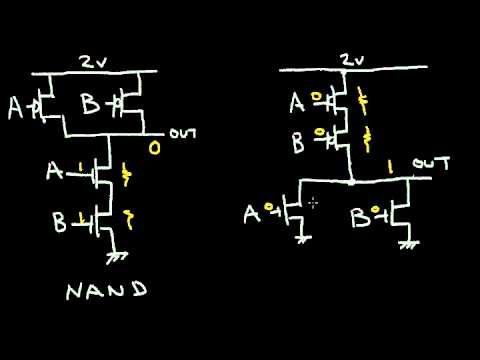
The CMOS NAND and NOR Gate
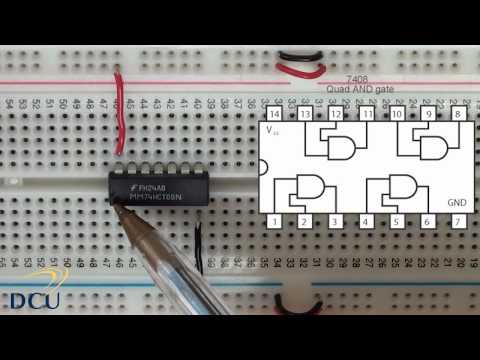
CD4073 | 3 input AND Gate CMOS logic IC