Via-in-Pad Design | PCB Knowledge
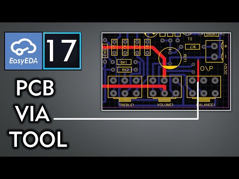
How to use Easy EDA Via Tool Class= 17 Urdu\Hindi
What are Stitching Vias? | PCB Knowledge
JLCPCB, Easyeda 5 tips for better PCB design
Copper Regions in EasyEDA
How and When to Use Via Stitching
Quick Tips [PCB 5]: Blind & Buried Vias
(Sponsored) PCB Vias 101 - Phil's Lab #77
3.10 PCB Copper Pour
EasyEDA 完全チュートリアル + コンポーネントの作成 + ヒント
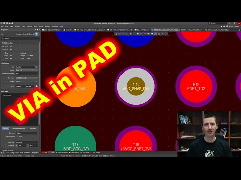
Using VIA in PAD? What you need to know - Guidelines, dimensions and more ...
How to Design a PCB from Scratch with EasyEDA | COMPLETE Tutorial | JLCPCB LCSC ALIEXPRESS | 2024
Handling DRC rules and adding new DRC rules using EasyEDA
Stitching Via Deep Dive | PCB Layout
Etching PCB At Home #shorts
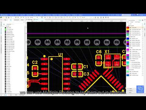
PCB - Route - Auto Router
3.8 PCB Routing Skill
How and When to Use Ground Fills
Learn PCB Designing Just in 15 Minutes! EasyEDA + JLCPCB Complete Tutorial 2023
最高のPCB設計ソフトウェアと最悪のPCB設計ソフトウェア