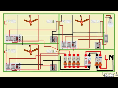
complete electrical house wiring diagram
wiring diagram layout diagram installation diagram circuit wiring diagram technical helper wiring
layout diagram
Stick diagram of a Boolean function || Explore the way
Layout of CMOS INVERTER using P-WELL Process || Explore the way
Calculation of area from Layout/Stick Diagram(VLSI)
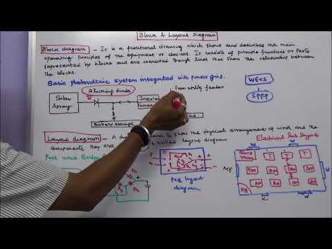
ELECTRICAL DIAGRAMS - PART – 03 - DIFFERENCE BETWEEN BLOCK AND LAYOUT DIAGRAM
CMOS inverter | Layout diagram | VLSI | Lec-33
SMTC की सच्चाई स्टूडेंट की जुबानी |
Design of CMOS Inverter Layout Diagram using Microwind Software | CMOS Inverter | Layout Diagram
Schematic diagram and layout of 2:1 multiplexer
Layout of 2-input CMOS NAND gate || P-WELL process || Explore the way
iPhone X HD Components Layout Diagram
Interpreting a Network Diagram
CMOS logic functions | Layout diagram | VLSI | Lec-35
Schematic diagram and layout of transmission gate
Diagram Layout in Sparx Systems Enterprise Architect
Wiring layout | wiring diagram | Wiring layout For house | wiring layout diagram | වයරින් සැලසුම
CMOS 2-input NAND and NOR gates | Layout diagram | VLSI | Lec-34
LAYOUT DIAGRAM OF MEDIUM DEPOSIT TUNNEL