How to draw 2 input NAND gate layout in Microwind
CMOS 2-input NAND and NOR gates | Layout diagram | VLSI | Lec-34
Cadence Virtuoso:: Layout of NAND Gate || Part-2.
cmos NANDゲートのレイアウト設計 | CMOS VLSI マスク レイアウト
2 input NAND gate stick and mask layout design using cmos technology, How to design stick and mask
Design of CMOS NAND Gate Layout Diagram using Microwind Software | CMOS NAND | NAND Layout Diagram
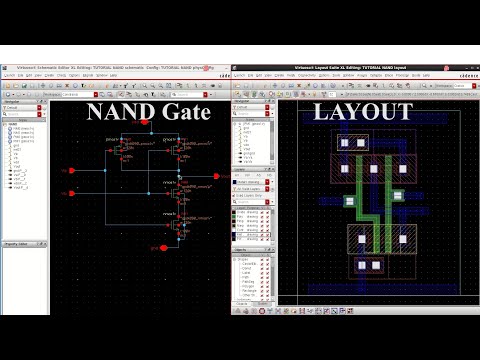
NAND Gate Schematic & Layout.
Design of CMOS NAND Gate Layout Diagram using Microwind Software as per circuit| NAND Layout Diagram
CMOS NOR Gate Layout Design | NOR gate layout | NAND gate Layout
Microwind での NAND ゲートの設計
stick diagram of two input CMOS nand gate || compact stick diagram || Explore the way
Layout of 2-input CMOS NAND gate || P-WELL process || Explore the way
CMOS NAND Gate Layout - Tutorial 4
CMOS INTEGRATED CIRCUIT DESIGN AND FABRICATION - NAND GATE LAYOUT USING L EDIT SOFTWARE
Layout of two input NAND gate in Magic
18EC72 MODULE2 LAYOUT DIAGRAM PART 2
Calculation of area from Layout/Stick Diagram(VLSI)
STICK DIAGRAM of 2 input NAND gate in CMOS Design Style
Layout diagram of 2 inputCMOS NAND GATE.
Layout design of Two input NAND logic using Microwind